Photovoltaic wafers trace their origin to semiconductor ingots, and for a long time the industry followed semiconductor wafer diameters of 6 and 8 inches — corresponding to edge lengths of 125 mm and 156 mm. As cell equipment improved and output demands grew, 125 mm wafers were progressively retired; after 2012 the size was essentially obsolete apart from one or two specialised manufacturers.
The first deliberate fine-tuning came in 2015, when mono wafer makers moved the edge length from 156.00 mm to 156.75 mm and reduced the chamfer, producing the M2 wafer. That revision was ratified by the SEMI standards committee in 2017, effectively unifying mono and multi wafers at 156.75 mm; China's national multi-crystalline standard likewise adopted 156.75 mm in its 2018 revision and recommended that future changes step in 1 mm multiples.
The unification did not last. Seeking maximum efficiency and power at existing module sizes to qualify for China's Top Runner programme, manufacturers introduced 157.0, 157.3, 157.5, 157.75 and 158.0 mm variants. Driven by the goal of exceeding 400 W per module and by the wish to minimise line modifications, sizes such as 158.75, 161.75 and 166 mm followed. Larger wafers and cells reduce per-watt processing cost from wafer to cell to module, so increasing size is a genuine direction of technical progress — but the resulting diversity forces wafer producers to build special sizes that cannot be sold to other customers, creates inventory and waste, leaves some cells without buyers, and prevents equipment suppliers from committing to next-generation platforms. Since 2017, under IEC TC82/WG8, major wafer, cell, module, equipment and testing organisations have worked together on a standard geometry for crystalline-silicon wafers used in PV cell production, covering Czochralski mono, cast multi and cast-mono material, recommending widely used sizes and giving guidance on future dimensions. Through discussion and voting, three sizes were selected as industry-recommended standards: 156.75 mm, 158.75 mm and 166.00 mm.
The guiding principles are pragmatic rather than technical: no size is inherently better than another, and a recommended size is simply one most companies will accept. The number of specifications should be kept as small as possible; changes smaller than 1.0 mm above an established size — typically made to squeeze the most out of a particular module format while minimising equipment modification — should be actively discouraged; new sizes achievable by substantially upgraded lines should be spaced far enough apart to be meaningful and accepted by module users; a modest increment should be reserved to guide future growth; and for quasi-square wafers the ingot diameter should be recommended rather than mandated.

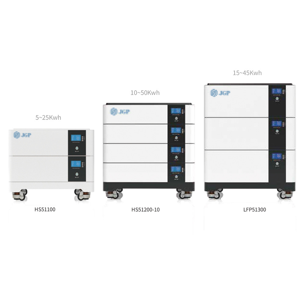 磷酸铁锂储能电池(5kWh~50kWh 可堆叠 / 移动式)磷酸铁锂 LiFePO4
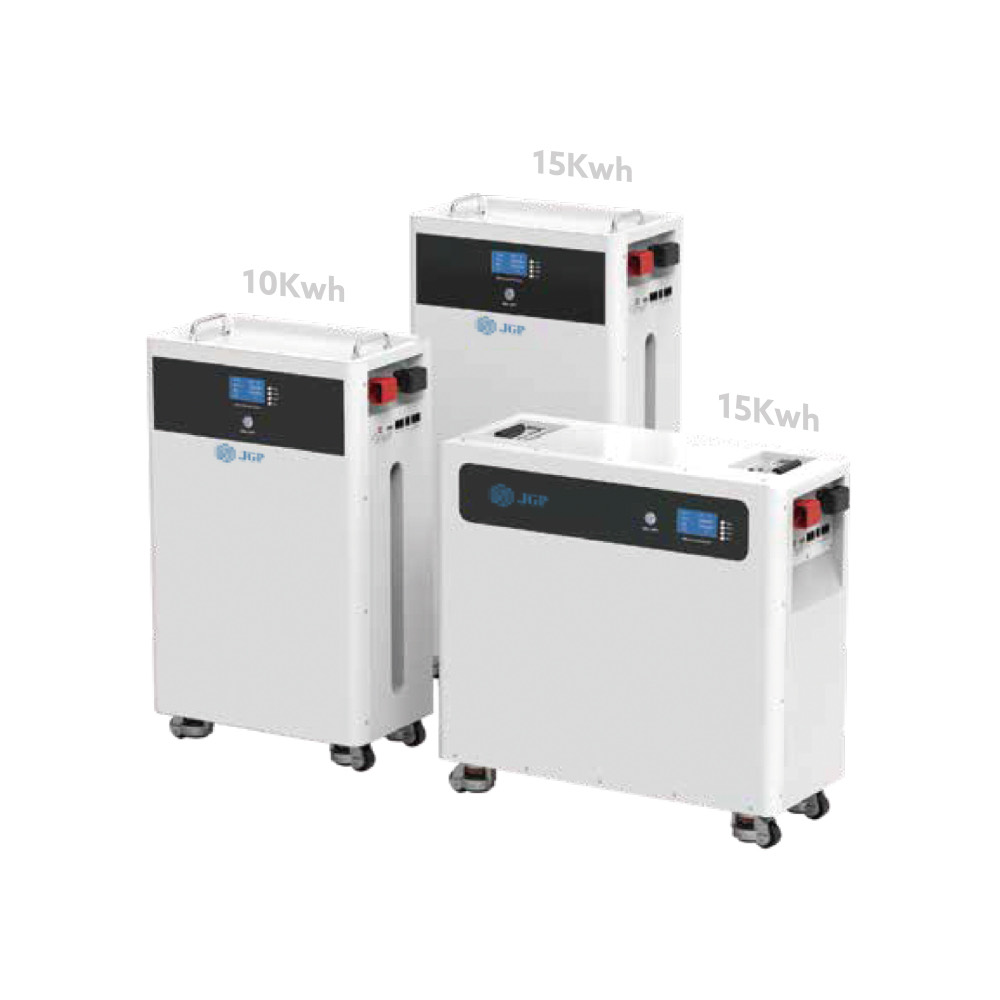 磷酸铁锂储能电池(10kWh~15kWh 可移动式)磷酸铁锂 LiFePO4
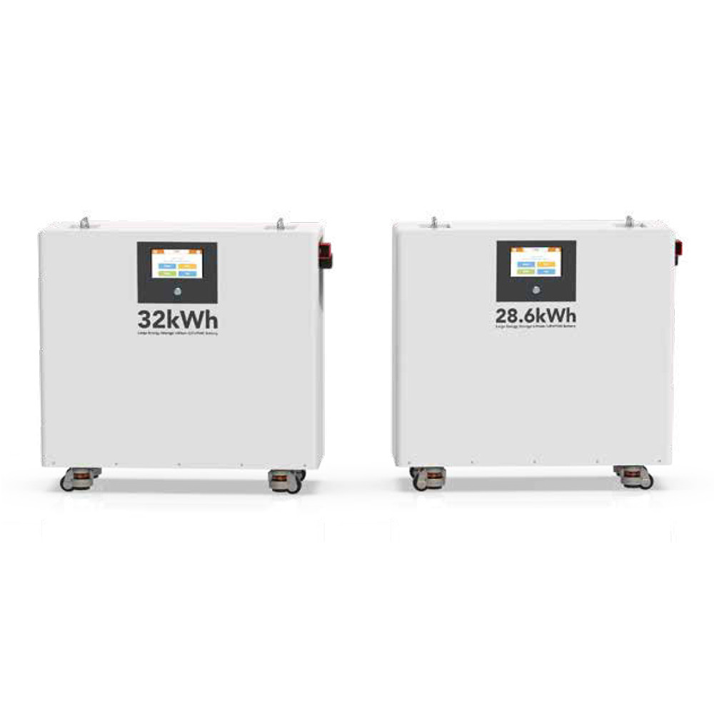 磷酸铁锂储能电池(28.6kWh~32kWh 可移动式)磷酸铁锂 LiFePO4
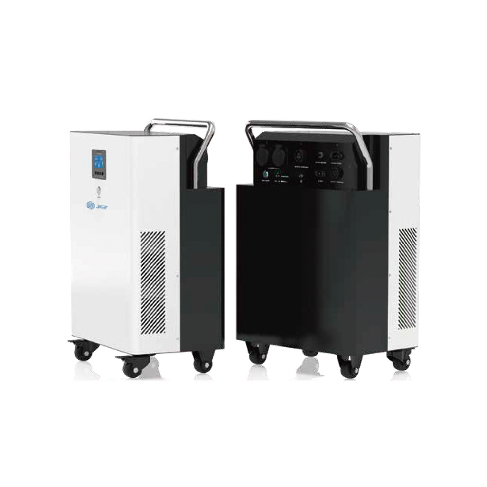 移动式便携电站(5kWh 电池 + 5kW 逆变器)磷酸铁锂 LiFePO4
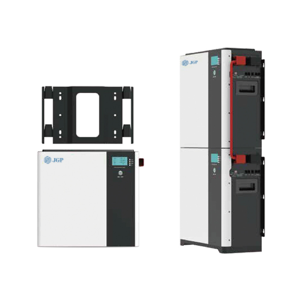 磷酸铁锂储能电池(2.5kWh~20kWh 壁挂可堆叠)磷酸铁锂 LiFePO4
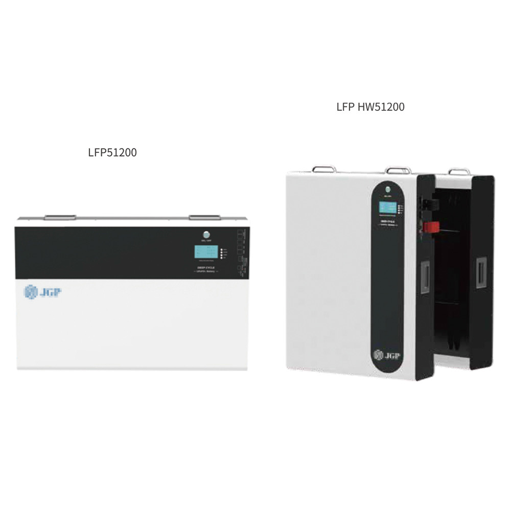 磷酸铁锂储能电池(10kWh 壁挂系列)磷酸铁锂 LiFePO4
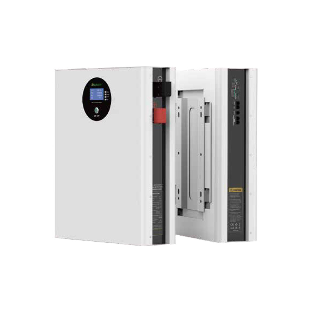 固态电池(5kWh 壁挂系列)磷酸铁锂 LiFePO4
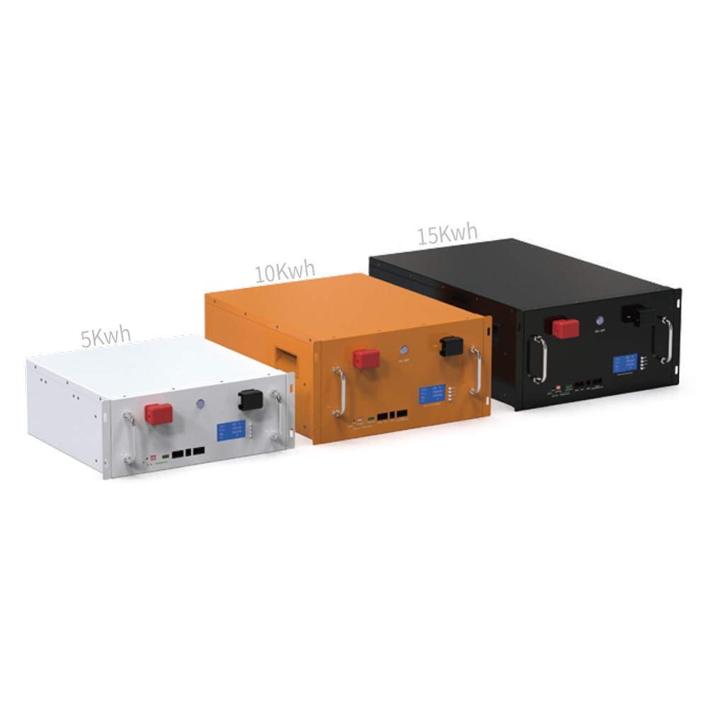 磷酸铁锂储能电池(5kWh~15kWh 机架式系列)磷酸铁锂 LiFePO4
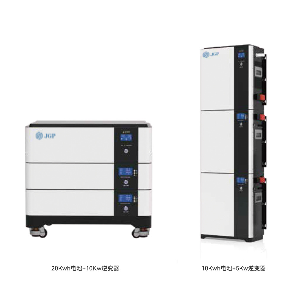 一体化混合储能系统(储能电池 + 5kW / 10kW 逆变器)磷酸铁锂 LiFePO410钠离子电池组(48V / 51.2V 系列)48 V / 51.2 V11锂离子电池组与电芯(18650 / 聚合物 / 定制)18650 packs / Polymer packs / LiFePO4 packs查看全部产品 →